- Home Page
- Company Profile
-
Our Products
- Advanced Nano Materials
- Carbon Nanofibers (CNFs)
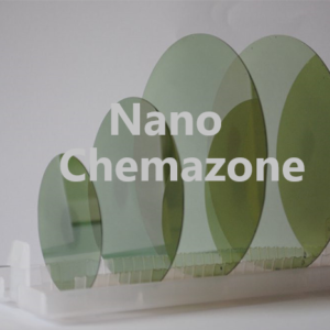
- Monolayer Tungsten Disulfide
- Tungsten Disulfide
- Nano Size Monolayer Tungsten Disulfide
- Monolayer Molybdenum Disulfide
- Black Phosphorus Powder
- Black Phosphorus Crystal
- Molybdenum Disulfide Powder, MoS2
- MOLYBDENUM DISULFIDE (MOS2) QUANTUM DOTS
- Graphitic Carbon Nitride (g-C3N4) Powder
- Hexagonal Boron Nitride (H-BN) on Copper Foil
- Hexagonal Boron Nitride (H-BN) on Si/SiO2
- Tungsten Disulfide (WS2)
- Nano Size Monolayer Tungsten Disulfide, WS2
- Monolayer Tungsten Disulfide Powder, WS2
- Monolayer Tungsten Disulfide (WS2) Quantum Dots
- Alloys
- ALUMINIUM MAGNESIUM ALLOY NANOPOWDER
- Nickel Zinc Iron Oxide Alloy Powder
- Aluminium Alloy Nanopowder
- Aluminium Alloy Powder
- Silicon Aluminium Alloy Nanopowder
- Lanthanum Nickel Alloy Nanopowder
- COPPER SILVER ALLOY NANOPOWDER
- HAFNIUM CARBIDE POWDER
- Tin Copper Alloy Powder
- Iron Nickel Cobalt Alloy Nanopowder
- Lanthanum Iron Palladium Alloy Nanopowder
- COPPER TIN ALLOY NANOPOWDER
- INCONEL 625 NICKEL ALLOY NANOPOWDER
- COBALT CHROMIUM MOLYBDENUM ALLOY POWDER
- Magnesium Calcium Alloy Powder
- Manganese Zinc Alloy Nanopowder
- Zirconia Toughened Alumina Alloy Powder
- Cobalt Iron Alloy Powder
- COPPER NICKEL ALLOY NANOPOWDER
- COPPER CHROMIUM ALLOY NANOPOWDER
- Tin Copper Alloy Powder / Nanopowder
- Titanium Aluminium Vanadium Alloy Powder
- Tin Lead Alloy Nanoparticles
- COPPER BERYLLIUM ALLOY NANOPOWDER
- Iron Nickel Alloy Nanopowder
- DEVARDA ALLOY POWDER
- Silver Copper Alloy Nanoparticles
- Zirconium Palladium Alloy Powder
- COPPER ZINC ALLOY NANOPARTICLES
- Iron Pyrite Powder
- Aluminium Casting Alloy Powder
- Iron Pyrite Alloy Nanopowder
- Iron Silicon Alloy Nanopowder
- Neodymium Iron Boron Nanoparticles
- Nickel Chromium Cobalt Alloy Nanopowder
- Aluminium Alloy Powder
- Molybdenum Disilicide Powder
- Lanthanum Cerium Zirconate powder
- Lanthanum Hafnium Zirconate powder
- Application Oriented Materials
- Artificial Biological Solutions
- Carbon Nanotube and Fullerene
- Functionalized SWCNT-Single Walled Carbon Nanotubes
- Short Length Single Walled Carbon Nanotubes (SWCNT)
- Functionalized Short MWCNT-Multi Walled Carbon Nanotubes
- Functionalized Short MWCNT-Multi Walled Carbon Nanotubes
- Multi Walled Carbon Nanotubes (MWCNT)
- Short Length Multi Walled Carbon Nanotubes (MWCNT)
- Carbon Nanotubes (Multi and Single Walled)
- SWCNT-Single Walled Carbon Nanotubes
- Core Shell Nano and Micro Structures
- Blue Luminescent Graphene Quantum Dots
- Cobalt Silica Core Shell Nanoparticles
- Iron Nickel Silica Core Shell Nanoparticles
- Gold Silver Core Shell Nanoparticles
- Iron Oxide Silica Core Shell Nanoparticles
- Zinc sulfur Manganese Silica Core Shell Nanoparticles
- Nickel Silica Core Shell Nanoparticles
- Gold Silicon Oxide Core-Shell Nanoparticles
- Silver Silica Core Shell Nanoparticles
- ZnO SiO2 Core Shell Nanoparticles
- Copper Silica core/shell Nanoparticles
- Silica Core Shell Nanoparticles
- AgI Silica Core Shell Nanoparticles
- Aluminium Silicon Oxide Core Shell Nanoparticles
- Silver Silica Core Shell Nanoparticles
- Gold Cadmium Selenium Core Shell Nanoparticles
- Iron Oxide Silicon Dioxide Titanium Oxide Core Shell
- Gold Copper Iodide Core Shell Nanoparticles
- Gold Cobalt Core Shell Nanoparticles
- Gold Platinum Core Shell Nanoparticles
- Au TiO2 Core Shell Nanoparticles
- Cadmium Selenide Cadmium Sulfur Silica Core Shell NPs
- IRON OXIDE SILICA CORE SHELL NANOPARTICLES
- Iron Nickel Silica Core Shell Nanoparticles
- Gold Platinum Core Shell Nanoparticles
- Dispersions Nano and Micro
- Epoxycyclohexyl POSS {(C8H13O)n(SiO1.5)n 99.99%}
- Iron Oxide Nanoparticles Dispersion (Fe2O3, Purity: 99.9 %, APS: 20-100 nm)
- Swcnt Dispersion (>95%, Diameter: 1-2 Nm, Length: 5-10 Um)
- Zinc Nanoparticles Dispersion (Zn, Purity: 99.99 %, Aps: 50 Nm)
- Calcium Carbonate Dispersion (Caco3, Purity: 99.99%, Aps: <80 Nm)
- Bismuth Oxide Dispersion (Bi2O3, Purity: 99%)
- Silver Dispersion Nanoparticles (Ag, Colloidal, Purity: 99.9%, APS: 150nm)
- Zirconium Oxide Nanoparticle Dispersion (ZrO2, Purity: 99.9 %, APS: 45-55 nm)
- Europium Doped Zinc Oxide Dispersion
- Antimony Tin Oxide Dispersion (Ato, Sno2:Sb2O3=90:10, 20 Wt%, 20-80 Nm)
- Alumina Slurry Polishing Dispersion
- Gallium Nanoparticles Dispersion
- Aluminium Dispersion (Al, Purity: 99.99 %, Aps: 80 Nm)
- Octaphenyl Silsesquioxane Dispersion (Octaphenyl POSS, Purity: 99.99%)
- Yttrium Doped Zinc Oxide Dispersion (Y/ZnO, 99.9%, APS: 50 nm)
- Carbon Nano Fiber Dispersion Organic Solvent
- Silica Dispersion (SiO2, Aqueous Dispersion, Amorphous; 5-35 nm)
- Niobium Doped Titanium Dioxide Dispersion (Nb/TiO2, IPA, 99.9%, 2-5 m)
- Titanium Dioxide Dispersions Cosmetic (TiO2, Rutile, 99.9 %, 30-50 nm)
- Octa Ammonium POSS (C24H72Cl8N8O12Si8, 98.0%)
- Niobium Powder with MPS Ligand (Purity: >99.99%, APS: 80-100 nm)
- Copper Nanoparticles Ink Dispersion
- Aluminum Powder Dispersion
- Alumina Dispersion (Al2O3 Dispersion)
- Barium Sulfate Dispersion (Baso4, 99%, 200-500 Nm)
- Copper Nanoparticles Dispersion
- Aluminium Oxide Dispersion (Al2O3, Gamma, 99.99 %, 20-30 Nm)
- Gold Nanoparticles Dispersion (Au, Purity: 99.99%, APS: <10 nm)
- Cerium Oxide Nanoparticle Dispersion
- Octamethyl POSS (Octamethylsilsesquioxane, Purity: 99.99%)
- Octavinyl Poss (Octavinyloctasilasesquioxane, Purity: 99.99%)
- Titanium Dioxide Nanoparticles Dispersion (Tio2, Rutile, 99.9 %, 15-30 Nm)
- Zno Nanoparticle Dispersion (Zinc Oxide, 99.9%, 30-40 Nm)
- Platinum Dispersion (Pt, Purity: 99.99%, Aps: 1-10 Nm)
- Zinc Oxide Slurry Dispersion (Zno, Purity: 99.9%, Aps: 50-80 Nm)
- Niobium Nanopowder Dispersion with EDA Ligand (Purity: >99.9%, APS: 80-100 nm)
- Carbon Nanofiber Dispersion In Water ( Length: 30 Um)
- Swcnt Water Dispersion (>95%, Diameter: 1-2 Nm, Length: 5-15 Um)
- Graphene Dispersion Organic Solvent (C, Purity: >98%, Hydrophobic)
- Magnesium Nanoparticle Dispersion (Mg, Purity: 99.99 %, APS: 80 nm)
- MWCNT Dispersion (Organic Solvent, Diameter: 20-30 nm, Length: 5-15 um)
- Nickel Oxide Dispersion (Nio, Butanol, Purity: 99.9 %, Aps: 50 Nm)
- Zinc Copper Core Shell Dispersion (Zncu, Purity: 99.99% Aps: 40 Nm)
- Zirconia Slurry Polishing (Zro2, Purity: 99.9 %, Aps: 50-80 Nm)
- Silicon Dioxide Dispersion (SiO2, Aqueous Dispersion, Amorphous)
- Carbon Conductive Ink Dispersion ( Purity: 99.9%, Aps: 80-100 Nm)
- Transparent Conductive Ink Dispersion
- Silver Copper Alloy Dispersion (Ag:cu, Purity: 99.9 %, Aps: <80 Nm)
- Silver Colloidal Dispersion (Ag, Colloidal, Purity: 99.99%, APS: 20nm)
- Aluminium Powder Dispersion (Al, Purity: 99.99 %, Aps: 80 Nm)
- Copper Zinc Alloy Nano Dispersion (Zn Cu, Purity: 99.99%, APS: 50 nm)
- Boron Nitride Nanoparticles Dispersion (Bn, Aps: 80-100 Nm)
- Silver Nano Water Dispersion (Ag, Purity: 99.99%, APS: <80nm)
- Electrodes Films Wafers and Targets
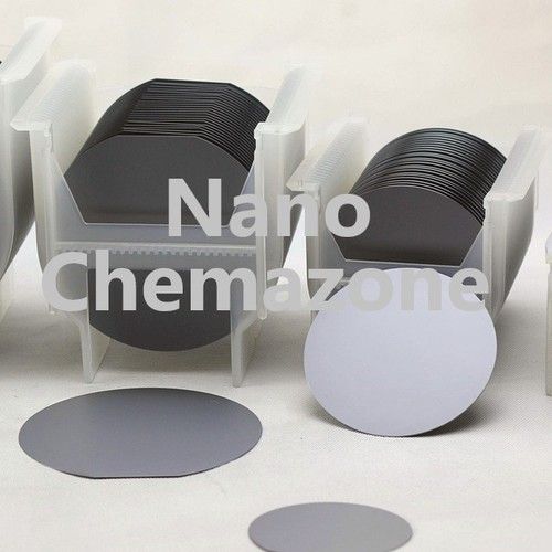
- N Doped Silicon Wafer (4 inch N Type Phosphorus Doped)
- Germanium Wafers
- Microcrystalline Cellulose Wafer
- Zensor Screen Printed Electrodes
- Sapphire Wafer C Plane (Al2O3)
- Silicon Carbide Wafers N-Type (Phosphorus Doped)
- Platinum Coated Silicon Wafer
- Silicon Germanium Wafers
- Silicon Wafers ( Doped and Undoped)
- Silicon Wafer with Silicon Dioxide Layer
- Platinum And Gold Coated Silicon Wafer
- Silicon Wafer Undoped
- Nanostructured Carbon Screen Printed Electrodes
- Silicon Wafer 6 inch (P Type, Boron Doped)
- Electrode
- Rectangular Mesh Tem Grids - Gold
- Zensor Screen Printed Electrodes
- Glassy Carbon Electrode (GCE)
- Square Mesh Grids - Palladium
- Rectangular Mesh Tem Grids - Copper
- Rectangular Mesh Tem Grids - Nickel
- Rectangular Mesh Tem Grids - Nickel
- Square Mesh Grids - Nickel
- Square Mesh Grids - Gold
- Parallel bar grids - Copper
- Square Mesh Grids - Gold
- Rectangular Mesh Tem Grids - Copper
- Rectangular Mesh Tem Grids - Palladium
- Gold Screen Printed Electrodes
- Platinum Screen Printed Electrode
- Silver Screen Printed Electrode
- Wafers
- BORON DOPED SILICON WAFER
- Microcrystalline Cellulose Wafer
- Doped Silicon Wafer
- SILICON WAFER SILICON DIOXIDE LAYER
- SILICON WAFER UNDOPED
- SAPPHIRE WAFERS
- N DOPED SILICON WAFER
- SILICON WAFER 6 INCH
- Industrial SILICON GERMANIUM WAFERS
- COATED SILICON WAFER GOLD/SILVER/PLATINUM/CHROMIUM
- GERMANIUM WAFER
- SILICON CARBIDE WAFERS
- Foams Foils and Coatings
- INDIUM TIN OXIDE COATED GLASS (ITO)
- INDIUM TIN OXIDE COATED GLASS (ITO)
- INDIUM TIN OXIDE COATED GLASS (ITO)
- INDIUM TIN OXIDE COATED GLASS (ITO)
- INDIUM TIN OXIDE COATED GLASS (ITO)
- INDIUM TIN OXIDE COATED GLASS (ITO)
- INDIUM TIN OXIDE COATED GLASS (ITO)
- Fluorine Doped Tin Oxide coated Glass
- Fluorine Doped Tin Oxide coated Glass
- Fluorine Doped Tin Oxide coated Glass
- Fluorine Doped Tin Oxide coated Glass
- Fluorine Doped Tin Oxide coated Glass
- INDIUM TIN OXIDE COATED GLASS (ITO)
- INDIUM TIN OXIDE COATED GLASS (ITO)
- Indium Tin Oxide coated Glass (ITO)
- INDIUM TIN OXIDE COATED GLASS (ITO)
- INDIUM TIN OXIDE COATED GLASS (ITO)
- INDIUM TIN OXIDE COATED GLASS (ITO)
- Fluorine Doped Tin Oxide coated Glass
- Aluminium Foams
- INDIUM TIN OXIDE COATED GLASS (ITO)
- INDIUM TIN OXIDE COATED GLASS (ITO)
- Fluorine Doped Tin Oxide coated Glass
- Fluorine Doped Tin Oxide coated Glass
- Fluorine Doped Tin Oxide coated Glass
- Fluorine Doped Tin Oxide coated Glass
- INDIUM TIN OXIDE COATED GLASS (ITO)
- INDIUM TIN OXIDE COATED GLASS (ITO)
- INDIUM TIN OXIDE COATED GLASS (ITO)
- INDIUM TIN OXIDE COATED GLASS (ITO)
- INDIUM TIN OXIDE COATED GLASS (ITO)
- Foils
- Metalic Foams
- Graphene Nano Structure
- Reduced Graphene Oxide Powder
- Graphene Water Solution
- BLUE LUMINESCENT GRAPHENE QUANTUM DOTS
- 1.0-1.5 wt% Graphene
- AMINATED GRAPHENE QUANTUM DOTS
- Graphene on Lacey Carbon 300 Mesh Copper TEM Grids
- Graphene on Ultra-Fine 2000 Mesh Copper TEM Grids
- Graphene Nanoplatelets Powder
- Graphene on Silicon Nitride TEM Grids
- Graphene Oxides
- Graphene Powder
- Graphene Sheet
- 0.4-0.5 wt% Graphene
- Graphene on Ultra-Flat Thermal SiO2 Substrate
- Graphene Nanoplatelets Industrial Grade (Graphene Nanoplatelets
- 3D Freestanding Graphene Foam
- Carboxylated Graphene Quantum Dots
- CVD Graphene on SiO2 Substrate
- CVD Graphene on Silicon Substrate
- CVD GRAPHENE ON PET SUBSTRATE
- 3D FREESTANDING GRAPHENE FOAM
- 3D GRAPHENE ON NICKEL/COPPER FOAM
- CARBOXYLATED GRAPHENE QUANTUM DOTS
- 5 wt% (Graphene Nanoplatelets & Carbon Nanotubes) Water/NMP Dispersion
- CVD Graphene on Quartz Substrate
- CVD Graphene on PET Substrate
- Graphene Nanoplatelets
- Nitrogen-doped Graphene
- Reduced Graphene Oxide
- Cvd Graphene on Copper Foil
- CVD Graphene on Quartz Substrate
- CVD Graphene on SiO2 Substrate
- Hydroxylated Graphene Quantum Dots
- Pretreated Graphene-PMMA Coated
- CVD Graphene
- Graphene and Graphene Oxide
- Graphene Nanoplatelets
- Graphene Quantum Dots
- Micro Particles and Powders
- Bronze powder
- Molybdenum Pentachloride (Molybdenum Chloride, MoCl5, 99%)
- Manganese Powder
- Iron Micropowder
- Zirconium Powder
- Silicon Nitride Powder
- Silicon Powder
- Niobium Micropowder
- Copper Powder
- Graphite Powder
- Chromium Powder
- Tantalum Powder
- Gold Powder
- Bilirubin Powder
- SULPHUR POWDER RED AR GRADE
- Boron Powder
- MAGNESIUM POWDER
- Nickel Powder
- COBALT MICRO POWDER
- Aluminium Powder
- Mesoporous Carbon Materials
- Zinc Powder
- Mesoporous Carbon Materials
- SILVER POWDER
- Bismuth (III) Sulfide Powder
- Niobium Pentachloride Powder
- Vanadium Micro Powder
- Stainless Steel Powders
- Neodymium Iron Boron Magnetic Powder (NdFeB)
- Soft Iron Powder
- Manganese Carbonate Micro Particles Powder
- Niobium Micro Powder
- Palladium Powder
- Brass Powder
- Milled Carbon Fiber Powder
- Cadmium Powder
- Transparent Conductive Ink
- Bismuth Powder
- Titanium Powder
- Tin Powder
- Bismuth Aluminium Powder
- MOF
- Europium Metal Organic Framework
- Dysprosium Metal Organic Framework
- Iron Metal Organic Framework
- Chromium Metal Organic Framework
- Methylimidazole Zinc Salt MOF
- Tin Metal Organic Framework
- Nanoporous Iron Metal Organic Frameworks (MIL-89)
- Aluminium Metal Organic Framework
- Metal Organic Framework
- Terbium Metal Organic Framework
- Manganese Metal Organic Framework
- Samarium Metal Organic Framework
- Zinc Based Metal Organic Framework (Zn (MOF-177), Purity: 99%, APS: 30-40um)
- Titanium Metal Organic Framework (NH2-MIL-125 (Ti), Purity: 99%, APS: 30-40um)
- Ferrous Metal Organic Framework (MIL-53)
- Nickel Based Metal Organic Framework
- Aluminium Metal Organic Framework (Al-MIL-53)
- Vanadium Metal Organic Frameworks (V-MIL-47, Purity: 99%, APS: 30-40um)
- Copper Metal Organic Framework
- Zirconium Metal Organic Framework
- Nano Particles and Nano Powders
- Cerium oxide nanoparticles
- Gold Nanoparticles
- Copper Nanoparticles
- Bismuth Nanopowder
- Chromium Oxide Nanopowder
- Carbon Nanopowder
- Diamond Nanoparticles
- Europium Oxide Nanoparticles
- Aluminum Nitride (AlN, 99.9 %, less than 100 nm)
- Copper oxide nanoparticles
- Dysprosium Oxide Nanoparticles
- Cobalt Nanoparticles
- Zirconium Oxide Powder with Less Hafnium Content
- Cobalt Ferrite Nanoparticles
- Tantalum Nitride Nanoparticles
- Graphene Nanoplatelets Powder
- Tin nanoparticles powder
- Cadmium Selenide Nanoparticles
- Zinc Nanoparticles
- Cadmium Sulfide Nanoparticles
- Alumina Nanoparticles Powder
- Aluminium Hydroxide Nanoparticles
- Silver Nanoparticles
- Chromium carbide nanoparticles
- Silicon Powder Spherical
- Manganese Zinc Alloy Nanopowder
- Erbium Oxide Nanoparticles
- Hafnium Oxide Nanoparticles
- Aluminum Nanoparticles (Al, > 99.9%, 50 nm)
- Aluminum Oxide Nanoparticles (Al2O3, alpha, 99.9%, 200 nm)
- Antimony tin oxide nanoparticles 99.99% 10 nm powder
- Barium Iron Oxide (BaFe12O19, 99.9 %, 200 nm)
- Barium Sulfate (BaSO4, 99 %, 200-500 nm)
- Barium Titanate Nanoparticles (BaTiO3, cubic, 99.9 %, 100 nm)
- Boron carbide nanoparticles (B4C, 99.9 %, 500 nm)
- Boron nitride nanoparticles
- Boron Oxide Nanoparticles
- Boron Oxide Nanoparticles
- Calcium carbonate nanoparticles powder
- Gadolinium Oxide Nanoparticles
- Graphite nanoparticles
- Indium Hydroxide Nanoparticles
- Indium Oxide Nanoparticles
- Indium Tin Oxide ITO Nanoparticles
- Iron Nanoparticles
- Iron Oxide Hydroxide Goethite Nanoparticles
- Iron oxide nanoparticles
- Iron oxide nanoparticles powder
- Lanthanum Oxide Nanoparticles
- Magnesium Hydroxide Nanoparticles
- Magnesium Oxide Nanoparticles
- Molybdenum Nanoparticles
- Molybdenum Oxide Nanoparticles
- Neodymium Oxide Nanoparticles
- Nickel Nanoparticles
- Nickel oxide nanoparticles
- Platinum Nanoparticles
- Titanium Nanoparticles
- Titanium Oxide Nanoparticles Anatase
- Titanium Oxide Nanoparticles Rutile
- Tungsten Oxide Nanoparticles
- Cadmium Oxide Nanoparticles
- Cadmium Nanopowder
- Silica Coated Aluminium Nano powder
- Aluminum Nitride Nanoparticles
- Aluminum Oxide Nanoparticles
- Antimony Oxide Nanoparticles
- Barium Iron Oxide Nanoparticles
- Barium Sulfate (BaSO4) Nanoparticles
- Barium Titanate
- Chromium Nanoparticles
- Zinc Oxide Nanoparticles
- Yttrium Oxide nanoparticles
- Tungsten Nanoparticles
- Ytterbium Fluoride Nanoparticles
- Tungsten Carbide Cobalt Nanoparticles
- Nanorods
- Nano Wires
- Hydroxyapatite Nanowire
- Nickel Hydroxide Nanowire
- Zinc Oxide Nanowire
- Iron Nanowires
- Titanium Dioxide Nanowire
- Manganese Tungstate Nanowire
- Silicon Carbide Nanowire
- Lead Zirconate Titanate Nanowire
- Hydroxyapatite Nanowire
- Aluminium Oxide Nanowires
- Manganese Oxide Nanowires
- Titanium Dioxide Nanowire
- Silicon Nanowire on Silicon Wafer Substrate
- Vanadium Oxide Nanowires
- Nickel Nanowires
- Copper Nanowire
- Cobalt Nanowires
- Nickel Oxide Nanowire
- Tellurium Nanowire
- Titanium Oxide Anatase Nanowires
- Magnesium Oxide Nanowire
- Tungsten Oxide Nanowire
- Iron oxide Nanowires
- Lead Nanowires
- Lead Titanate Nanowires
- Gold Nanowire
- Highly Conducting Silver Nanowire
- Lanthanum Oxide Nanowires
- Iron Oxyhydroxide Nanowires
- Potassium Trimolybdate Nanowire
- Silver Nanowires (Ag Nanowires)
- Copper Hydroxide Nanowires
- Sodium Ammonium Tri Molybdate Nanowires
- Coating and Membrane Grade Titanium Oxide Nanowires
- Carbon films on Nickel Grids
- Carbon Films on Nickel Grids
- Quantum Dots
- Indium Phosphide/Zinc Sulphide Quantum Dots (InP/ZnS) QUANTUM DOTS
- Cadmium Telluride Quantum Dots
- INP ZNS QUANTUM DOTS
- LED Quantum Dots (Zinc Selenide /Zinc Sulphide Quantum Dots)
- Carbon COOH QDs
- Blue Luminescent Hydrophobic Graphene Quantum Dots (Powder)
- Blue Luminescent Hydrophilic Graphene Quantum Dots (Powder)
- Zinc Selenide /Zinc Sulphide Quantum Dots
- Molybdenum Disulfide Quantum Dots
- Cadmium Sulphide Quantum Dots
- Blue Luminescent Hydrophilic Graphene Quantum Dots
- Blue Luminescent Hydrophobic Graphene Quantum Dots
- Cadmium Sulphide /Zinc Sulphide Quantum Dots
- ZnCdSeS alloyed Quantum Dots
- LED Quantum Dots
- CdSe ZnS Quantum Dots
- Graphene Quantum Dots Powder
- Upconverting Nanoparticles
- Paste & Inks
- Dielectric Paste for Screen Printing Electrode
- Silver-Palladium Conducting Paste
- Platinum Gold Conductor Paste
- Carbon Graphene Screen Print Ink Paste
- Copper Paste
- Tungsten Conducting Paste
- Silver Platinum Conductor Paste
- Titanium Dioxide Paste
- Silver/Silver Chloride Pastes for Electrochemistry
- Silver Paste
- Silver Conducting Paste
- Conducting Gold Paste
- Nickel Oxide Anode Paste
- Platinum Conducting Paste
- Yttria Stabilized Zirconia Paste
- Gold Paste for Screen Printing
- Platinum Paste Screen Print Ink
- Carbon Screen Print Paste and Ink
- Aluminum Oxide Paste
- Insulating Paste for Screen Printing
- Tungsten Conductor Paste
- Speciality Chemicals & Materials
- AZO COATED GLASS
- PVDF Powder Poly(vinylidene fluoride)
- Polyketone Powder
- Wafer Tweezers Type 46WF
- MOF-801 (Zr) Powder MOF
- Serialised Rotary Grid Storage Box for 25 grids (Pk10)
- Zr2SnC Max Phase Powder
- Chitosan Powder
- PCN-600 (Fe) Powder MOF
- Leit C Thinners (30ml)
- Silicon Wafer, chips 5 x 5 mm. (Approx 270 chips per wafer)
- INDIUM TIN OXIDE COATED GLASS (ITO)
- Pinnatoxin-G CAS: 1312711-74-2
- Graphene oxide support film on Lacey carbon on 400mesh Cu grids (pack of 25)
- Carbon films on Copper Grids
- Carbon Type-B 300 mesh Pack of 50
- Carbon Films on 400 Mesh Grids Copper (Pack of 50)
- Fluorine Doped Tin Oxide coated Glass
- Rotary Grid Storage Box Kit with Dumont N5AC Tweezers
- Fluorine Doped Tin Oxide coated Glass
- INDIUM TIN OXIDE COATED GLASS (ITO)
- Hydrothermal Autoclave Reactor
- Lacey Carbon Films on 300 Mesh Copper Grids (Pack of 25)
- Grid storage box with identification number
- INDIUM TIN OXIDE COATED GLASS (ITO)
- Carbon Films on 300 Mesh Gold Grids (Pack of 50)
- AZO COATED GLASS
- FTO Coated Glass
- Grid storage box for 96 grids
- Hydrothermal Autoclave Reactor
- Fluorine Doped Tin Oxide coated Glass
- Hydrothermal Autoclave Reactor
- Grid storage box for 100 grids
- Agar Grids 300 Mesh Copper 3.05mm (Tube of 100)
- Graphene Oxide Powder
- INDIUM TIN OXIDE COATED GLASS (ITO)
- Silver Tin Alloy Powder
- Silver Platinum Alloy Powder
- Cobalt Iron Alloy Powder (Nano and Micron Particle Size)
- INDIUM TIN OXIDE COATED GLASS (ITO)
- Indium Tin Oxide Coated Glass
- Hexagonal mesh grids - Nickel
- Adhesive Carbon Tape 8mm x 20m
- Fluorine Doped Tin Oxide coated Glass
- INDIUM TIN OXIDE COATED GLASS (ITO)
- Fluorine Doped Tin Oxide coated Glass
- INDIUM TIN OXIDE COATED GLASS (ITO)
- Sodium hypochlorite
- Hexagonal mesh grids - Copper
- Hydrothermal Autoclave Reactor
- Titanium Aluminium Vanadium Ti-6Al-4V powder spherical
- Leit C Conducting Carbon Cement (30ml)
- Carbon Films on 200 Mesh Gold Grids (Pack of 50)
- AZO Coated Glass
- Fluorine Doped Tin Oxide coated Glass
- Zirconium Oxide Powder with Less Hafnium Content
- Holey Carbon Films on 300 Mesh Copper Grids (Pack of 50)
- AZO COATED GLASS
- Grid storage box
- INDIUM TIN OXIDE COATED GLASS (ITO)
- INDIUM TIN OXIDE COATED GLASS (ITO)
- Lacey Carbon Films on 400 Mesh Copper Grids (Pack of 50)
- INDIUM TIN OXIDE COATED GLASS (ITO)
- Fluorine Doped Tin Oxide coated Glass
- INDIUM TIN OXIDE COATED GLASS (ITO)
- Carbon Films on 300 Mesh Grids Copper (Pack of 25)
- INDIUM TIN OXIDE COATED GLASS (ITO)
- Aluminium Nitride
- INDIUM TIN OXIDE COATED GLASS (ITO)
- INDIUM TIN OXIDE COATED GLASS (ITO)
- Lacey Carbon Films on 300 Mesh Copper Grids (Pack of 50)
- Wafer Tweezers Type 8WF
- Ti3C2Tx MXene Few-Layer Dispersion Solution
- Type 92 Polyimide Film Tape - 12mm x 33m
- Fluorine Doped Tin Oxide coated Glass
- Fluorine Doped Tin Oxide coated Glass
- Carbon films on Copper Grids
- INDIUM TIN OXIDE COATED GLASS (ITO)
- Agar Grids 200 Mesh Gold Centre mark 3.05mm (Tube of 50)
- AZO COATED GLASS
- Carbon Films on 300 Mesh Grids Copper (Pack of 50)
- Fluorine Doped Tin Oxide coated Glass
- Lacey Carbon Films on 200 Mesh Copper Grids (Pack of 50)
- Carbon Films on 400 Mesh Grids Copper (Pack of 25)
- Agar Grids 300 Mesh Gold 3.05mm (Tube of 50)
- Holey Carbon Films on 200 Mesh Copper Grids (Pack of 50)
- Wafer Tweezers Type 4WL
- Carbon Tape with Aluminium 8mm x 20m
- Short Length MWCNT-Multi Walled Carbon Nanotubes
- Holey Carbon Films on 300 Mesh Copper Grids (Pack of 25)
- INDIUM TIN OXIDE COATED GLASS (ITO)
- Copper Foil Conductive Tape
- Formvar/Carbon on 300 Mesh Copper (Pack of 50)
- Fluorine Doped Tin Oxide coated Glass
- INDIUM TIN OXIDE COATED GLASS (ITO)
- Fluorine Doped Tin Oxide Coated Glass
- Formvar/Carbon on 200 Mesh Copper (Pack of 50)
- Formvar/Carbon on 400 Mesh Copper (Pack of 50)
- Agar Grids 200 Mesh Copper Centre mark 3.05mm (Tube of 100)
- Fluorine Doped Tin Oxide coated Glass
- Fluorine Doped Tin Oxide coated Glass
- Parallel bar grids - Copper
- Parallel bar grids - Copper
- Parallel Bar Grids -Palladium
- Parallel Bar Grids -Palladium
- Parallel Bar Grids -Palladium
- Parallel Bar Grids -Palladium
- Folding Grids - Copper
- Folding Grids - Copper
- Folding Grids - Palladium
- Folding Grids - Palladium
- Folding Grids - Nickel
- Folding Grids - Nickel
- Folding Grids - Gold
- Hexagonal mesh grids - Nickel
- Hexagonal mesh grids - Nickel
- Hexagonal mesh grids - Nickel
- Hexagonal mesh grids - Nickel
- Hexagonal mesh grids - Nickel
- Hexagonal mesh grids - Gold
- Hexagonal mesh grids - Gold
- Hexagonal mesh grids - Gold
- Hexagonal mesh grids - Gold
- Hexagonal mesh grids - Gold
- Hexagonal mesh grids - Gold
- Hexagonal mesh grids - Gold
- Triple Slot Grid
- Single Hole TEM Grids - Copper
- Single Hole TEM Grids - Palladium
- Single Hole TEM Grids - Copper/Palladium
- Single Hole TEM Grids - Nickel
- Special Single Hole TEM Grids -Nickel
- Premium Single Hole TEM Grids -Nickel
- Single Hole TEM Grids -Nickel
- Particle Analysis Grids Copper
- Single Hole TEM Grids - Gold
- Single Hole TEM Grids -gold
- Tabbed grids - Copper
- Tabbed grids - Nickel
- Tabbed grids - gold
- Special Metal grids - Aluminium
- Special Metal grids - Aluminium
- Special Metal grids - Aluminium
- Special Metal grids - Aluminium
- Special Metal grids - Aluminium
- Special Metal grids - Molybdenum
- Special Metal grids - Molybdenum
- Special Metal grids - Molybdenum
- Special Metal grids - Molybdenum
- Special Metal grids - Molybdenum
- special metal grids -Molybdenum
- Special Metal Grids-Molybdenum
- Special Metal grids-Molybdenum
- Special Metal Grids-Molybdenum
- Special Metal grids - Molybdenum
- Special Metal grids - Molybdenum
- Special Metal grids - Molybdenum
- Special Metal grids - Stainless Steel
- Special Metal grids - Stainless Steel
- Industrial Special Metal Grids - Titanium
- Special Metal grids - Titanium
- Special Metal Grids -Titanium
- Special Metal Grids - Titanium
- Special Metal Grids - Titanium
- Special Metal Grids - Titanium
- Special Metal Grids - Titanium
- Finder Grids - 200 Mesh (6 grid)
- Abrasive Strips - Aluminium Oxide
- Abrasive Strips - Aluminium Oxide
- Abrasive Strips - Aluminium Oxide
- Abrasive Strips - Aluminium Oxide
- Abrasive Strips - Aluminium Oxide
- Abrasive Strips - Aluminium Oxide
- Industrial Abrasive Strips - Aluminium Oxide
- Speciality Abrasive Strips - Aluminium Oxide
- Abrasive strips - Aluminium Oxide
- Abrasive strips - Aluminium Oxide
- Abrasive strips - Aluminium Oxide
- Abrasive Strips - Aluminium Oxide Chemical
- Abrasive strips - Aluminium Oxide
- Abrasive strips - Aluminium Oxide
- Abrasive strips - Aluminium Oxide
- Abrasive strips - Aluminium Oxide
- Abrasive strips - Aluminium Oxide
- Abrasive Strips - Aluminium Oxide
- Abrasive Strips - Diamond
- Abrasive Strips - Diamond
- Abrasive Strips - Diamond
- Abrasive Strips - Diamond
- Abrasive Strips - Diamond
- Abrasive Strips - Diamond
- Abrasive Strips - Diamond
- Abrasive Strips - Diamond
- Abrasive Strips - Diamond
- Abrasive Strips - Diamond
- Abrasive Strips - Diamond
- Abrasive Strips - Diamond
- Abrasive Strips - Diamond
- Abrasive Strips - Diamond
- Abrasive Strips - Diamond
- Abrasive Strips - Diamond
- Abrasive Strips - Diamond
- Abrasive Strips - Diamond
- Abrasive Strips - Diamond
- Carbon films on Copper Grids
- Carbon films on Copper Grids
- Carbon films on Copper Grids
- Carbon films on Copper Grids
- Carbon films on Copper Grids
- Carbon films on Copper Grids
- Carbon films on Copper Grids
- Carbon films on Copper Grids
- Carbon films on Copper Grids
- Carbon films on Copper Grids
- Carbon films on Copper Grids
- Carbon films on Copper Grids
- Carbon films on Copper Grids
- Carbon films on Nickel Grids
- Carbon films on Nickel Grids
- Carbon films on Nickel Grids
- Carbon films on Nickel Grids
- Carbon films on Nickel Grids
- Carbon films on Nickel Grids
- Carbon films on Nickel Grids
- Carbon films on Nickel Grids
- Carbon films on Nickel Grids
- Carbon films on Nickel Grids
- Carbon films on Nickel Grids
- Carbon films on Nickel Grids
- Carbon films on Gold Grids
- Carbon films on Gold Grids
- Carbon films on Gold Grids
- Carbon films on Gold Grids
- Carbon films on Gold Grids
- Carbon films on Gold Grids
- Carbon films on Gold Grids
- Carbon films on Gold Grids
- Carbon films on Gold Grids
- Carbon films on Gold Grids
- Carbon films on Gold Grids
- Ultra-thin carbon support film, 3nm
- Ultra-thin carbon support film, 3nm
- Ultra-thin carbon support film, 3nm - on lacey carbon
- Stainless Steel Mesh 150mm x 150mm
- Lacey Carbon Films on 200 Mesh Copper Grids (Pack of 50)
- Lacey Carbon Films on 200 Mesh Copper Grids (Pack of 25)
- Lacey Carbon Films on 300 Mesh Copper Grids (Pack of 50)
- Lacey Carbon Films on 300 Mesh Copper Grids (Pack of 25)
- Lacey Carbon Films on 400 Mesh Copper Grids (Pack of 50)
- Lacey Carbon Films on 400 Mesh Copper Grids (Pack of 25)
- Lacey Carbon Films on H7 finder grid. Copper (Pack of 50)
- Lacey Carbon Films on H7 finder grid. Copper (Pack of 25)
- Lacey Carbon Films on 200 Mesh Nickel (Pack of 50)
- Lacey Carbon Films on 200 Mesh Nickel (Pack of 25)
- Lacey Carbon Films on 300 Mesh Nickel (Pack of 50)
- Lacey Carbon Films on 300 Mesh Nickel (Pack of 25)
- Lacey Carbon Films on 400 Mesh Nickel (Pack of 50)
- Lacey Carbon Films on 400 Mesh Nickel (Pack of 25)
- Lacey Carbon Films on H7 finder grid. Nickel (Pack of 50)
- Lacey Carbon Films on H7 finder grid. Nickel (Pack of 25)
- Lacey Carbon Films on 200 Mesh Gold (Pack of 50)
- Lacey Carbon Films on 200 Mesh Gold (Pack of 25)
- Lacey Carbon Films on 300 Mesh Gold (Pack of 50)
- Lacey Carbon Films on 300 Mesh Gold (Pack of 25)
- Lacey Carbon Films on 400 Mesh Gold (Pack of 50)
- Lacey Carbon Films on 400 Mesh Gold (Pack of 25)
- Lacey Carbon Films on H7 finder grid. Gold (Pack of 50)
- Lacey Carbon Films on H7 finder grid. Gold (Pack of 25)
- Holey Carbon Films on 200 Mesh Copper Grids (Pack of 50)
- Holey Carbon Films on 200 Mesh Copper Grids (Pack of 25)
- Holey Carbon Films on 300 Mesh Copper Grids (Pack of 50)
- Holey Carbon Films on 300 Mesh Copper Grids (Pack of 25)
- Holey Carbon Films on 400 Mesh Copper Grids (Pack of 50)
- Holey Carbon Films on 400 Mesh Copper Grids (Pack of 25)
- Holey Carbon Films on H7 Finder Grids Copper (Pack of 50)
- Holey Carbon Films on H7 Finder Grids Copper (Pack of 25)
- Holey Carbon Films on 200 Mesh Nickel (Pack of 50)
- Holey Carbon Films on 200 Mesh Nickel (Pack of 25)
- Holey Carbon Films on 300 Mesh Nickel (Pack of 50)
- Holey Carbon Films on 300 Mesh Nickel (Pack of 25)
- Holey Carbon Films on 400 Mesh Nickel (Pack of 50)
- Holey Carbon Films on 400 Mesh Nickel (Pack of 25)
- Holey Carbon Films on H7 Finder Grids Nickel (Pack of 50)
- Holey Carbon Films on H7 Finder Grids Nickel (Pack of 25)
- Holey Carbon Films on 200 Mesh Gold (Pack of 50)
- Holey Carbon Films on 200 Mesh Gold (Pack of 25)
- Holey Carbon Films on 300 Mesh Gold (Pack of 50)
- Holey Carbon Films on 300 Mesh Gold (Pack of 25)
- Holey Carbon Films on 400 Mesh Gold (Pack of 50)
- Holey Carbon Films on 400 Mesh Gold (Pack of 25)
- Holey Carbon Films on H7 Finder Grids Gold (Pack of 50)
- Holey Carbon Films on H7 Finder Grids Gold (Pack of 25)
- Formvar on 3mm 75 Mesh Cu Grids (Pack of 25)
- Formvar on 3mm 100 Mesh Cu Grids (Pack of 25)
- Formvar on 3mm 200 Mesh Cu Grids (Pack of 25)
- Formvar on 3mm 300 Mesh Cu Grids (Pack of 25)
- Formvar on 3mm 400 Mesh Cu Grids (Pack of 25)
- Formvar on 3mm F1 Finder Cu Grids (Pack of 25)
- Formvar on 3mm H7 Finder Cu Grids (Pack of 25)
- Formvar on 3mm 75 Mesh Ni Grids (Pack of 25)
- Formvar on 3mm 100 Mesh Ni Grids (Pack of 25)
- Formvar on 3mm 200 Mesh Ni Grids (Pack of 25)
- Formvar on 3mm 300 Mesh Ni Grids (Pack of 25)
- Formvar on 3mm 400 Mesh Ni Grids (Pack of 25)
- Formvar on 3mm F1 Finder Ni Grids (Pack of 25)
- Formvar on 3mm H7 Finder Ni Grids (Pack of 25)
- Formvar on 3mm 100 Mesh Au Grids (Pack of 25)
- Formvar on 3mm 200 Mesh Au Grids (Pack of 25)
- Formvar on 3mm 300 Mesh Au Grids (Pack of 25)
- Formvar on 3mm 400 Mesh Au Grids (Pack of 25)
- Formvar on 2mm x 1mm Au Slot Grids (Pack of 25)
- Formvar on 3mm F1 Finder Au Grids (Pack of 25)
- Formvar on 3mm H7 Finder Au Grids (Pack of 25)
- Formvar/Carbon on 75 Mesh Copper (Pack of 50)
- Formvar/Carbon on 75 Mesh Copper (Pack of 25)
- Formvar/Carbon on 200 Mesh Copper (Pack of 50)
- Formvar/Carbon on 200 Mesh Copper (Pack of 25)
- Formvar/Carbon on 300 Mesh Copper (Pack of 50)
- Formvar/Carbon on 400 Mesh Copper (Pack of 25)
- Formvar/Carbon on 2mmx1mm Slot Copper Grids (Pack of 50)
- Formvar/Carbon Films on F1 Copper Grids (Pack of 50)
- Formvar/Carbon Films on F1 Copper Grids (Pack of 25)
- Formvar/Carbon Films on Copper H7 Grids (Pk 50)
- Formvar/Carbon Films on Copper H7 Grids (Pack of 25)
- Formvar/Carbon on 75 Mesh Nickel (Pack of 50)
- Formvar/Carbon on 75 Mesh Nickel (Pack of 25)
- Formvar/Carbon on 100 Mesh Nickel (Pack of 50)
- Formvar/Carbon on 100 Mesh Nickel (Pack of 25)
- Formvar/Carbon on 100 Mesh Nickel (Pack of 25)
- Formvar/Carbon on 200 Mesh Nickel (Pack of 25)
- Formvar/Carbon on 300 Mesh Nickel (Pack of 50)
- Formvar/Carbon on 400 Mesh Nickel (Pack of 50)
- Formvar/Carbon on 400 Mesh Nickel (Pack of 25)
- Formvar/Carbon on 2mm x 1mm Nickel Slot (Pack of 50)
- Formvar/Carbon on 2mmx1mm Nickel Slot (Pack of 25)
- Formvar/Carbon Films on F1 Nickel Grids (Pack of 25)
- Formvar/Carbon Films on F1 Nickel Grids (Pack of 50)
- Formvar/Carbon Films on H7 Nickel Grids (Pack of 50)
- Formvar/Carbon Films on H7 Nickel Grids (Pack of 25)
- Formvar/Carbon on 75 Mesh Gold (Pack of 25)
- Formvar/Carbon on 100 Mesh Gold (Pack of 50)
- Formvar/Carbon on 100 Mesh Gold (Pack of 25)
- Formvar/Carbon on 200 Mesh Gold (Pack of 50)
- Formvar/Carbon on 200 Mesh Gold (Pack of 25)
- Formvar/Carbon on 300 Mesh Gold (Pack of 50)
- Formvar/Carbon on 300 Mesh Gold (Pack of 25)
- Formvar/Carbon on 400 Mesh Gold (Pack of 50)
- Formvar/Carbon on 400 Mesh Gold (Pack of 25)
- Formvar/Carbon on 2mmx1mm Gold Slots (Pack of 50)
- Formvar/Carbon on 2mmx1mm Gold Slots (Pack of 25)
- Formvar/Carbon Films on F1 Gold Grids (Pack of 50)
- Formvar/Carbon Films on F1 Gold Grids (Pack of 25)
- Formvar/Carbon Films on H7 Gold Grids (Pack of 50)
- Formvar/Carbon Films on H7 Gold Grids (Pack of 25)
- Graphene oxide support film on Lacey carbon on 400mesh Cu grids (pack of 25)
- Graphene oxide support film on Quantifoil R2/2 on 300mesh Cu grids (pack of 10)
- Quantifoil R1.2/1.3 Holey Carbon Films - Circular
- Quantifoil R1.2/1.3 Holey Carbon Films - Circular
- Quantifoil R1.2/1.3 Holey Carbon Films - Circular
- Quantifoil R2/1 Holey Carbon Films - Circular
- Quantifoil R2/1 Holey Carbon Films - Circularn
- Quantifoil R2/1 Holey Carbon Films - Circular
- Quantifoil R2/2 Holey Carbon Films - Circular
- Quantifoil R2/2 Holey Carbon Films - Circular
- Quantifoil R2/2 Holey Carbon Films - Circular
- Quantifoil R2/2 Holey Carbon Films - Circular
- Quantifoil R2/2 Holey Carbon Films - Circular
- Quantifoil R2/4 Holey Carbon Films - Circular
- Quantifoil R2/4 Holey Carbon Films - Circular
- Quantifoil R2/4 Holey Carbon Films - Circular
- UltrAuFoil Holey Gold Films
- Quantifoil R3.5/1 Holey Carbon Films - Circular
- Quantifoil R3.5/1 Holey Carbon Films - Circular
- Quantifoil R3.5/1 Holey Carbon Films - Circular
- Rotary Grid Storage Box for 25 grids
- Serialised Rotary Grid Storage Box for 25 grids
- Rotary Grid Storage Box for 25 grids (Pk10)
- Serialised Rotary Grid Storage Box for 25 grids (Pk10)
- Rotary Grid Storage Box Kit with Dumont N5AC Tweezers
- Rotary Grid Storage Box Kit with Dumont HP 5 SS Tweezers
- Metal Cryo Grid Box
- Metal Cryo Grid Box
- Rotary grid storage boxes for 6 TEM grids
- Grid storage boxes
- Grid storage boxes
- Grid storage box with identification number
- Grid storage box
- Grid storage box for 96 grids
- BEEM Dial-a-Grid Storage box
- Grid storage boxes
- Storage box for 50 tabbed grids
- Lift-out grid storage box
- FIB grid storage box
- Cryo TEM grid boxes
- Cryo TEM grid boxes
- Cryo Tem Grid Boxes
- Multicolour Cryo Grid Box Handling Rods
- Cryo Em Round Storage Box, 4 Hole, To Fit Fei Vitrobot
- Epoxim Cure
- Epoxi Cure
- Loctite 460 sample Bonding Adhesive, 50g.
- Epokwick Fast Curing Epoxy
- Epothin 2 Low Viscosity Epoxy
- Epothin 2 Low Viscosity Epoxy
- Specimen Mounting Wax
- Lacomit Varnish And Remover
- Diamond Polishing Paste Lubricant
- Kemet Diamond Polishing Paste
- Kemet Diamond Polishing Paste
- Kemet diamond polishing paste
- Abrasive Powders
- Ultraprep Diamond Lapping Films
- Scan-Dia Embedding System
- Wafer-Mount Adhesives
- Quickstick Temporary Mounting Wax, Pack Of 20
- Disposable Stirrers
- Polypropylene Cups
- Polypropylene Petri Dishes
- Polishing Cloths And Discs
- Abrasive strips - Diamond
- Abrasive strips - Aluminium Oxide
- INDIUM TIN OXIDE COATED GLASS (ITO)
- INDIUM TIN OXIDE COATED GLASS (ITO)
- Nafion-117 Solution
- Aluminium Boride Powder
- Iron Metal Powder
- Titanium Boride Powder
- Zirconium Boride Powder
- Aluminum Metal-Organic Framework
- Tin Metal Organic Frameworks
- Zinc Based Metal Organic Framework
- Mo2C MXenes Powder
- Ti2C MXene powder
- Ti3C2Tx (MXene) Powder
- Single walled Carbon Nanotubes
- Bentonite Nanoclay Powder
- Kaolin Nanoclay (Al2Si2O5 (OH)
- Clay Nanopowder Montmorillonite
- Aluminum Nanoparticles
- High-Density Polyethylene Powder
- Low-Density Polyethylene Powder
- Ultrafine Polyethylene Terephthalate Powder
- Poly(lactic acid) Powder
- Polypropylene Powder
- PTFE Nanopowder
- Carbon Micro Powder
- Aluminum Nitride Powder
- Viton Powder
- Cloisite 30B Nanoclay Powder
- Industrial Grade Graphene
- Titanium Boride Micro Powder
- Gold Palladium Core Shell Nano Particles
- Iridium Powder
- Aluminium Silicon Alloy Nanopowder
- Cadmium Selenide Silica Core Shell Nanoparticles
- Palladium Silver Alloy Nanopowder
- Mo3C2 MXene Powder
- Yttrium Oxide Powder
- Gold Iron Oxide Core Shell Nanoparticles
- Calcium Carbonate Silica Core Shell Nanoparticles
- Silicon Oxide Nanoparticles
- Titanium Nitride Powder
- Aluminium Manganese Alloy Powder
- Aluminium Nickel Alloy Nanopowder
- Neodymium Iron Boron Nano Particles
- Ti3C2Tx Mxene Few-Layer Dispersion Titanium Dioxide Solution
- H-BN Hexagonal Boron Nitride On Si/SiO2
- PR-601 PRASEODYMIUM OXIDE POWDER, Pr2O3
- Cadmium Selenide Cadmium Sulphur Silica Core Shell Nano Particles
- Magnesium Nitrate Powder
- Carbon Black Ink
- Ammonium Acetate Powder
- Osmium Powder
- Ruthenium Powder
- CARBON BLACK POWDER
- Copper Sulfate Powder
- Chlorine Dioxide
- Gold Wire
- Nitrogen Doped Graphene Powder
- Silicon Nitride Nanoparticles Powder
- Platinum Nanopowder
- Cobalt Oxide Nanoparticles
- Erbium Oxide Powder
- Calcium Carbonate Nanoparticles
- Diamond Powder
- Aluminium Oxide Nanoparticles
- Sodium Hexafluoroantimonate Powder
- Copper Sulphate Powder
- Copper Hydroxide Nano Wires
- Tin Oxide Nanoparticles Powder
- 3D Graphene on Nickel/Copper Foam
- Nickel Titanium Alloy Nanopowder
- Carbon Nanofiber Powder (CNFs)
- Cellulose Nanofiber Powder
- Calcium Oxide Nanoparticles
- Graphene Powder High Purity
- Graphene Powder Industrial Grade
- (R)-NOBIN MOF
- Aluminium Nickel Alloy Powder
- Carbon Activated Powder
- Silicon Dioxide Powder
- Cadmium Selenide Zinc Sulfur Silica Core Shell Nanoparticles
- Perovskite Quantum Dots
- Silver Iodide Silica Core Shell Nanoparticles
- Tin Lead Alloy Nanopowder
- MoAlB MAXene Powder
- Zirconium Dioxide Nanopowder
- Germanium Dioxide Powder
- Tungsten Carbide Powder
- Titanium Diboride Nanopowder
- Silicon Carbide Micro Powder
- Zinc Selenide Powder
- Zinc Sulfide Powder
- Ti3AlCN MAX Phase Powder
- V2AlN MAX Phase Powder
- Ti2SnC MAX Phase Powder
- Mo2AlC MAX Phase Powder
- TUNGSTEN METAL POWDER
- Neodymium Metal Powder
- Polystyrene Nanopowder
- Cellulose Nanoparticles
- Halloysite Clay Nanotubes
- Lithium Oxide Powder
- Nickel Aluminium Alloy Powder
- Lithium Cobalt Oxide Nanoparticles
- Zinc Chromate Nanopowder
- Niobium Nanoparticles
- Sodium Borohydride Powder
- Lithium Hydroxide Monohydrate
- Zirconium Silicate Powder
- Copper Conductor Paste
- Polyetheretherketone (PEEK)
- Nickel Iron Oxide Nanoparticles
- Titanium Dioxide Powder
- Zirconium Diboride
- Molybdenum Powder
- High Density Polyethylene Powder (HDPE)
- Low Density Polyethylene Powder (HDPE)
- Nylon Powder
- Poly Aniline Powder
- Poly Propylene Powder
- Poly Styrene Powder
- Poly Urethane Powder
- Poly(ether ketone ketone) PEKK Powder
- Poly(methyl methacrylate) PMMA Powder
- Polyaryletherketone (PAEK) Powder
- Polyester Powder
- Polyether Ether Ketone (PEEK) Powder
- Polyethylene Oxide (PEO) Powder
- Polyethylene Powder
- Polyethylene Terephthalate (PET) Powder
- Polylactic Acid (PLA) Powder
- Polytetrafluoroethylene (PTFE) Powder
- Polyvinyl Chloride (PVC) Powder
- Shape Memory Polymer Powder
- Polyphenylene Ether Powder
- Polyethersulfone (PES) Powder
- Fluoropolymer Powder
- Polyphenylene Sulfide (PPS) Powder
- Polyolefin Powder
- Polyetherimide (PEI) Powder
- Polyphthalamide (PPA) Powder
- Aluminum Silicon Carbide Max Phase Powder
- Cr2TiAlC Max Phase Powder
- Max Phase Aluminum Silicon Carbide Powder
- Max Phase Hafnium Carbide Silicon Nitride Powder
- Max Phase Manganese Aluminum Carbide Powder
- Max Phase Molybdenum Indium Carbide Powder
- Max Phase Nickel Aluminum Carbide Powder
- Max Phase Scandium Aluminum Carbide Powder
- Ruthenium Sponge Powder
- Max Phase Titanium Aluminum Nitride Powder
- Max Phase Titanium Germanium Carbide Powder
- Max Phase Vanadium Aluminum Carbide Powder
- Mo2Ti2C3 Max Phase Powder
- Mo2TiC Max Phase Powder
- Molybdenum Indium carbide Max Phase Powder
- Nickel Aluminum carbide Max Phase Powder
- Scandium Aluminum carbide Max Phase Powder
- Ti2VAlC2 Max Phase Powder
- Ti3SnC2 Max Phase Powder
- VCrAlC Max Phase Powder
- Chromium Carbide
- Chromium Nitride
- Cobalt-doped Titanium Aluminum Carbide
- Hafnium Carbonitride
- Zr2TIN Max Phase Powder
- Zr2TIC Max Phase Powder
- Zr2SC Max Phase Powder
- Zr2AIC Max Phase Powder
- V2GeC Max Phase Powder
- TiVAlC Maxene Powder
- Ti4AlN3 Maxene Powder
- Ti3GeC2 Maxene Powder
- Ti3C2 Mxene Quantum Dots
- Ti2TIC Max Phase Powder
- Ti2SiC Max Powder
- Ti2N Mxene Powder
- Ti2GeC Max Phase Powder
- Ti2GaN Max Phase Powder
- Ti2GaC Max Phase Powder
- Ti2Cdc Max Phase Powder
- Ti2AIN Max Phase Powder
- Ta4C3 Mxene Powder
- Ta4AlC2 Maxene Powder
- Ta2GaC Max Phase Powder
- Ta2AlC Maxene Powder
- Perhydroxyl Mxene Powder
- Nb4C3 Mxenes Powder
- Nb2SnC Max Phase Powder
- Nb2GaC Max Phase Powder
- Nb2AIC Max Phase Powder
- Mo2TiC2 Mxene Powder
- Mo2TiAlC2 Maxene Powder
- Mo2Ti2AlC3 Mxene Powder
- Mo2Gac Max Phase Powder
- Mn3AlC2 Maxene Powder
- Mn2GaC Max Phase Powder
- Hf2TIC Max Phase Powder
- Hf2SnN Max Phase Powder
- Hf2SnC Max Phase Powder
- Hf2SC Max Phase Powder
- Cr2GeC Max phase powder
- Cr2GaC Max phase powder
- Phenazine-1-carboxylic acid MOF
- Sodium tetrachloropalladate(II) Powder MOF
- COF-42 MOF
- COF-LZU-1 MOF
- CTF-1 MOF
- HCOF-1 MOF
- IISERP-COF4 MOF
- PyCOF MOF
- TpPa-1 MOF
- Melem MOF
- Potassium cyamelurate trihydrate MOF
- Geranyl linalool MOF
- Pyrene-1-carboxylic Acid MOF
- Tetrathiafulvalene MOF
- HOF-100 MOF
- HOF-102 MOF
- PFC-1 MOF
- 467-MOF (Al) Powder MOF
- Al-Fum Powder MOF
- Al-MIL-53-NH2 Powder MOF
- CAU-1-NH2 (Al) Powder MOF
- CAU-10 (Al) Powder MOF
- DUT-5 Powder MOF
- MIL-53 (Al) Powder MOF
- MIL-101(Al)-NH2 Powder MOF
- MOF-253 Powder MOF
- NH-MIL-101 (Al) Powder MOF
- PCN-333 (Al) Powder MOF
- ED-MIL-101 (Cr) Powder MOF
- MIL-53 (Cr) Powder MOF
- MIL-100 (Cr) Powder MOF
- MIL-101 (Cr)-SO3H Powder MOF
- NH2-MIL-101 (Cr) Powder MOF
- NO2-MIL-101 (Cr) Powder MOF
- Co-DOBDC Powder MOF
- DUT-8 (Co) Powder MOF
- ZIF-9 (Co) Powder MOF
- ZIF-67 Powder MOF
- CPL-1 Powder MOF
- CPL-2 Powder MOF
- CPL-5 Powder MOF
- DUT-8 (Cu) Powder MOF
- HKUST-1 Powder MOF
- HKUST-1(Cu) Powder MOF
- SIFSIX-1-Cu Powder MOF
- SIFSIX-2-Cu Powder MOF
- MIL-124 (In) Powder MOF
- MIL-53 (Fe) Powder MOF
- MIL-68 (Fe) Powder MOF
- MIL-88B-Fe Powder MOF
- MIL-100 (Fe) Powder MOF
- MIL-101 (Fe) Powder MOF
- NH2-MIL-53 (Fe) Powder MOF
- NH2-MIL-88B (Fe) Powder MOF
- NH2-MIL-101 (Fe) Powder MOF
- PCN-250 (Fe) Powder MOF
- DUT-8 (Ni) Powder MOF
- KAUST-7 Powder MOF
- Ni-DOBDC Powder MOF
- MIL-125 (Ti) Powder MOF
- NH2-MIL-125 (Ti) Powder MOF
- CAU-21-ODB Powder MOF
- IRMOF-3 Powder MOF
- IRMOF-8 Powder MOF
- IRMOF-9 Powder MOF
- MIL-96 (Al) Powder MOF
- MIL-100 (Al) Powder MOF
- MOF-5 Powder MOF
- MOF-74 (Mg) Powder MOF
- MOF-177 Powder MOF
- ZIF-7 Powder MOF
- ZIF-8 Powder MOF
- ZIF-11 Powder MOF
- ZIF-14 Powder MOF
- ZIF-64 Powder MOF
- ZIF-68 Powder MOF
- ZIF-69 Powder MOF
- ZIF-70 Powder MOF
- ZIF-90 Powder MOF
- Zn-ZIF-62 Powder MOF
- 2COOH-UIO-66 (Zr) Powder MOF
- MIP-202 (Zr)Powder MOF
- MOF-808 (Zr) Powder MOF
- MOF-867 Powder MOF
- NH2-UiO-66 Powder MOF
- NO2-UIO-66 Powder MOF
- NU-1000 (Zr) Powder MOF
- PCN-128 (Zr) Powder MOF
- PCN-222 (Fe) Powder MOF
- PCN-222 (H) Powder MOF
- PCN-223 (H) Powder MOF
- PCN-777 (Zr) Powder MOF
- UIO-66-(OH) 2 Powder MOF
- UIO-66-COOH Powder MOF
- PCN-224 (H) Powder MOF
- 1,4-Piperidinediylbis (oxy), 2,2,6,6-tetramethyl- Powder MOF
- 1-Piperidinyloxy, 2,2,6,6-tetramethyl-4-(2-oxiranylmethoxy)-Powder MOF
- TBTA Powder MOF
- Benzyl Benzodithioate MOF
- bis (benzylsulfanyl) methanethione Powder MOF
- Cumyl benzodithioate Powder MOF
- Cyanoisopropyl DithiobenzoatePowder MOF
- Cyanomethyl Dodecyl Trithiocarbonate Powder MOF
- Cyanomethylmethyl (phenyl) carbamodithioate Powder MOF
- Di (thiobenzoyl) disulfide Powder MOF
- Trithiocarbodiglycolic acid Powder MOF
- RARE EARTH METALS
- Yttrium Oxide (Y2O3) Micron Powder
- Dysprosium Oxide (Dy2O3) Micron Powder
- Lanthanum Trifluoride (LaF3) Nanopowder/Nanoparticles
- Lanthanum Aluminate (LaAlO) Powder Micron and Nano Size
- Lanthanum Hexaboride (LaB6) Micron Powder
- Yttrium Aluminate (Y3Al5O12) Nanopowder/Nanoparticles
- Cerium (Ce) Micron Powder
- Dysprosium (Dy) Micron Powder
- Erbium (Er) Micron Powder
- Europium (Eu) Micron Powder
- Gadolinium (Gd) Micron Powder
- Holmium (Ho) Micron Powder
- Lanthanum (La) Micron Powder
- Lutetium (Lu) Micron Powder
- Neodymium (Nd) Micron Powder
- Praseodymium (Pr) Micron Powder
- Samarium (Sm) Micron Powder
- Scandium (Sc) Micron Powder
- Terbium (Tb) Micron Powder
- Thulium (Tm) Micron Powder
- Ytterbium (Yb) Micron Powder
- Yttrium (Y) Micron Powder
- Cerium Oxide (CeO2) Micron Powder
- Cerium Oxide (CeO2) Nanopowder/Nanoparticles
- Dysprosium Oxide (Dy2O3) Nanopowder/Nanoparticles
- Erbium Oxide (Er2O3) Micron Powder
- Erbium Oxide (Er2O3) Nanopowder/Nanoparticles
- Europium Oxide (Eu2O3) Micron Powder
- Europium Oxide (Eu2O3) Nanopowder/Nanoparticles
- Gadolinium Oxide (Gd2O3) Micron Powder
- Gadolinium Oxide (Gd2O3) Nanopowder/Nanoparticles
- Holmium Oxide (Ho2O3) Micron Powder
- Lanthanum Oxide (La2O3) Micron Powder
- Lanthanum Oxide (La2O3) Nanopowder/Nanoparticles
- Lutetium Oxide (Lu2O3) Micron Powder
- Neodymium Oxide (Nd2O3) Micron Powder
- Neodymium Oxide (Nd2O3) Nanopowder/Nanoparticles
- Praseodymium Oxide (Pr6O11) Micron Powder
- Praseodymium Oxide (Pr6O11) Nanopowder/Nanoparticles
- Samarium Oxide (Sm2O3) Micron Powder
- Samarium Oxide (Sm2O3) Nanopowder/Nanoparticles
- Scandium Oxide (Sc2O3) Micron Powder
- Terbium Oxide (Tb4O7) Micron Powder
- Terbium Oxide (Tb4O7) Nanopowder/Nanoparticles
- Thulium Oxide (Tm2O3) Micron Powder
- Yttrium Oxide (Y2O3) Nanopowder/Nanoparticles
- Cerium (Ce) Micron Powder
- Dysprosium (Dy) Micron Powder
- MXene & MAXene Powder
- Ti3SiC2 MAXene Powder
- Titanium carbide (Ti3C2) MXene freestanding thin films
- Ti3C2Tx (MXene) Thin Layer Dispersion Solution
- Ti3AlC2 MAXene Powder
- V2C MXene Powder
- Mo3AlC2 MAXene Powder
- Ti3C2Tx MXene Few Layer Dispersion Solution
- Mn2AlC MAXene Powder
- Mo2Ga2C MAXene Powder
- V4AlC3 MAXene Powder
- Cr2AlC MAXene Powder
- Ti3AlC2 MXene
- V2AlC MAXene Powder
- Ti2AlC MAXene Powder
- Ti2C MXene Powder
- Nb2AlC MAXene Powder
- Ta4AlC3 MAXene Powder
- Ti3C2Tx (MXene) multilayer Nanoflake
- Nb4AlC3 MAXene Powder
- Nb2CTx MXene Multilayer Nanoflake
- Ti2AlC Ceramic Material
- Ti2AlN MAXene Powder
- Ti3C2Tx (MXene) Nanosize thin layer dispersion
- Ti3C2Tx (MXene) Thin Layer Dispersion Solution
- Ti3C2Tx MXene Few layer Nanoflake
- Artificial Perspiration
- Artificial Sweat
- Artificial Eccrine Perspiration - Not Stabilized (BZ110)
- Artificial Eccrine Perspiration - Stabilized (BZ112)
- Artificial Eccrine Perspiration - Stabilized 1000 ml (BZ113)
- Artificial Eccrine Perspiration - Stabilized 200ml (BZ111)
- Artificial Eccrine Perspiration Custom pH - Not Stabilized. 200ml (BZ114)
- Artificial Eccrine Perspiration Custom pH - Stabilized. 200ml (BZ115)
- ARTIFICIAL ECCRINE PERSPIRATION GMW14334 Sweat, 2-Part Alkaline Non-stabilized (BZ160)
- Artificial Eccrine Perspiration, Acidic, Custom pH, Stabilized (BZ157)
- Artificial Eccrine Sweat-Sebum Emulsion (BZ118)
- Artificial Eccrine Sweat-Sebum Emulsion, Refrigerated (BZ130)
- Artificial Perspiration - Custom pH, Not Stabilized ANSI-BHMA A156.18 (BZ142)
- Artificial Perspiration - Not Stabilized, ANSI-BHMA-A156.18 (BZ141)
- Artificial Perspiration DN 53160-2-BS EN 1811 (BZ125)
- Artificial Perspiration, AATCC TEST METHOD 15 Sweat - Custom pH, Not Stabilized (BZ138)
- Artificial Perspiration, AATCC TEST METHOD 15 Sweat - Custom pH, Stabilized (BZ139)
- Artificial Perspiration, AATCC Test Method 15 Sweat - not Stabilized (BZ135)
- Artificial Perspiration, AATCC TM 15 Sweat - Stabilized (BZ140)
- Artificial Perspiration, AATCC TM15 Sweat pH 4.3 Stabilized (BZ136)
- Artificial Perspiration, AATCC TM15 Sweat pH 4.3 Stabilized (BZ137)
- Artificial Perspiration, AATCC TM15 Sweat pH 4.3 Stabilized (BZ148)
- Artificial Perspiration, Alkaline, Custom pH. 200 ml (BZ156)
- Artificial Perspiration, Custom pH - Stabilized. (BZ129)
- Artificial Perspiration, GMW 14334, Alkaline, Non-Stabilized (BZ128)
- Artificial Perspiration, ISO 105-B07 Acidic solution - Not Stabilized (BZ151)
- Artificial Perspiration, ISO 105-B07 Acidic Solution - pH 5.5, Stabilized (BZ154)
- Artificial Perspiration, ISO 105-B07 Acidic, Custom pH (BZ155)
- Artificial Perspiration, ISO 105-B07 Alkaline Solution - Not Stabilized (BZ152)
- Artificial Perspiration, ISO 105-B07 Alkaline Solution - pH 8.0, Stabilized (BZ153)
- Artificial Perspiration, ISO 105-B07 Alkaline, Custom pH, Stabilized (BZ158)
- Artificial Perspiration, ISO 11641 Sweat - Custom pH, Not Stabilized (BZ145)
- Artificial Perspiration, ISO 11641 Sweat - Custom pH, Stabilized. 200ml (BZ146)
- Artificial Perspiration, ISO 11641 Sweat - Not Stabilized. 200ml (BZ143)
- Artificial Perspiration, ISO 11641 Sweat - Stabilized (BZ144)
- Artificial Perspiration, ISO 12870 Sweat - Custom pH, Not Stabilized (BZ149)
- Artificial Perspiration, ISO 12870 Sweat - Custom pH, Stabilized (BZ150)
- Artificial Perspiration, ISO 12870 Sweat - Not Stabilized (BZ147)
- Artificial Perspiration, ISO 3160 - Not Stabilized. 200ml (BZ123)
- Artificial Perspiration, ISO 3160 - Stabilized. (BZ127)
- Artificial Perspiration, ISO 3160 - Stabilized. 200ml (BZ124)
- BS EN 1811-2011, Artficial Perspiration Custom pH (BZ121)
- BS EN 1811-2011, Artficial Perspiration Stabilized (BZ120)
- BS EN 1811-2011, Artficial Perspiration, Custom pH, Stabilized (BZ122)
- D4265-14 Artificial Sebum - Not Stabilized (BZ116)
- D4265-14 Artificial Sebum - Stabilized (BZ117)
- DIN 53160-2-2010-10 Artificial Perspiration - Custom pH, Not Stabilized. 200ml (BZ133)
- DIN 53160-2-2010-10 Artificial Perspiration - Custom pH, Stabilized. 200ml (BZ134)
- DIN 53160-2-2010-10 Artificial Perspiration - Not Stabilized 200ml (BZ131)
- DIN 53160-2-2010-10 Artificial Perspiration - Stabilized 200ml (BZ132)
- DN 53160-2-BS EN 1811, Artificial Perspiration (BZ119)
- GMW14334 Sweat, Acidic Non-Stabilized (BZ159)
- Artificial Saliva
- Artificial Urine
- Artificial Urine for Corrosion Testing of Urological Implants, Non Stabilized (BZ101)
- Artificial Urine Medium for Growing Urological Pathogens (BZ103)
- Artificial Urine Stabilized (BZ104)
- Artificial Urine, Synthetic Urine, Simulated Urine (BZ186)
- DIN EN 1616-1999 Artificial Urine (BZ102)
- DIN EN 1616-1999 Artificial Urine (BZ102S), Stabilized
- Simulated Urine for Corrosion Testing of Urological Implants, Stabilized (BZ188)
- Simulated Fluid
- Artificial Amniotic Fluid BZ259
- Artificial Aqueous Humour Fluid (BZ276)
- Artificial Bone Marrow Fluid (BZ268)
- Artificial Brain Fluid (BZ256)
- Artificial Breast Milk (BZ255)
- Artificial Bronchoalveolar Lavage (BAL) Fluid (BZ305)
- Artificial Canine Saliva (BZ297)
- Artificial Cerebrospinal Solution (ACSF, Sterile) (BZ178)
- Artificial Cerumen (Not Stabilized) or Synthetic Earwax (BZ171)
- Artificial Cerumen (Stabilized) or Synthetic Earwax 50g (BZ172)
- Artificial Cholesterol Fluid (BZ265)
- Artificial Colonic Fluid (sterile) pH7.8 (BZ177)
- Artificial Colostrum Fluid (BZ306)
- Artificial Dandruff or Synthetic Dandruff (BZ293)
- Artificial Endosomal Body Fluid (BZ260)
- Artificial Feline Saliva or Cat Saliva (BZ301)
- Artificial gastric fluid (sterile) pH1.5 Simulated Gastric Fluid (SGF) -Sterile (BZ175)
- Artificial Intestinal Fluid (Sterile) pH6.8 Simulated Intestinal Fluid (SIF) -Sterile (BZ176)
- Artificial Luminal Fluid (BZ283)
- Artificial Lymph Fluid (BZ267)
- Artificial Lysosomal Fluid (BZ257)
- Artificial Menses Fluid (BZ266)
- Artificial Mucus Matrix (BZ275)
- Artificial Nasal Fluid (BZ251)
- Artificial Nasal Mucus (BZ253)
- Artificial Nasopharyngeal Fluid (BZ252)
- Artificial Otitis Media Fluid (BZ304)
- Artificial Peripheral Lymph Fluid (BZ303)
- Artificial Phlegm (BZ296)
- Artificial Plasma Fluid (BZ273)
- Artificial Pleural Fluid BZ258
- Artificial Renal Tubular Fluid (BZ269)
- Artificial Rhinorrhea (BZ295)
- Artificial Serum Ultrafiltrate (BZ307)
- Artificial Sputum Matrix (BZ274)
- Artificial Vomitus Fluid (BZ282)
- Artificial Wound Fluid Exudate (BZ292)
- Gamble's Solution Lung Fluid (BZ284)
- Hank's Balanced Salt Solution (BZ261)
- Modified-Simulated Body Fluid (Sterile) (BZ174)
- Phagolysosomal Simulant Fluid (PSF) (BZ262)
- SBF Simulated Body Fluid (Sterile) Simulated Body Fluid (BZ173)
- Simulated Baby Hands Sweat (BZ298)
- Simulated Bile Juice (BZ263)
- Simulated Blood Matrix (BZ281)
- Simulated Blood Serum (BZ278)
- Simulated Cochlear Fluid (BZ286)
- Simulated Duodenal Fluid (BZ299)
- Simulated Endolymph Fluid (BZ287)
- Simulated Extracellular Fluid (BZ280)
- Simulated Hepatic Fluid (BZ264)
- Simulated Inflammatory Fluid (SIF) (BZ302)
- Simulated Interstitial Fluid (BZ254)
- Simulated Interstitial Lung Fluid (SILF) (BZ300)
- Simulated Intrapleural Fluid (BZ290)
- Simulated Lung Fluid (BZ179)
- Simulated Pancreatic Juice (BZ271)
- Simulated Pericardial Fluid (BZ288)
- Simulated Perilymph Fluid (BZ285)
- Simulated Peritoneal Fluid (BZ289)
- Simulated Prostate Fluid (BZ272)
- Simulated Renal Fluid (BZ270)
- Simulated Semen Solution or Seminal fluids (BZ180)
- Simulated Serous Fluid (BZ291)
- Simulated Synovial Fluid (BZ183)
- Simulated Tears (BZ182)
- Simulated Transcellular Fluid (BZ279)
- Simulated Vaginal Fluid (SVF) (BZ181)
- Simulated Vitreous Humor (BZ277)
- Synthetic Fecal Stool (BZ308)
- Synthetic Vernix Caseosa (BZ294)
- Square Mesh Tem Support Grids
- Copper Products
- Advanced Nano Materials
- Contact Us